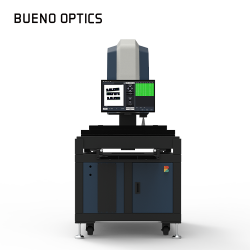
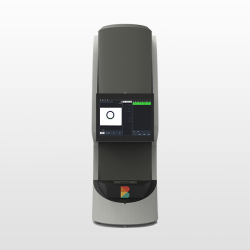
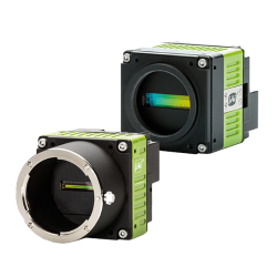
Intelligent Optical Wafer Surface Defect and Height Variation Inspection Equipment
Model: SE-5AT2
Category: Artificial Intelligence
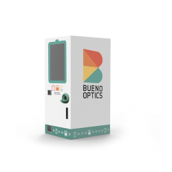
Exhibitor: BUENO OPTICS CO., LTD.
Booth No: L701
Characteristic
Provide accurate optical inspection and analysis for the defects generated in the semiconductor wafer manufacturing process.
Apply the microscope auto focus module and the XYZ axis displacement platform (integrated optical scale) to perform flying trigger to capture the wafer surface image.
The image comparison method and AI image deep learning method can be provided according to the defects that need to be detected, which can reduce the occurrence of overkill and underkill, automatically sort OK and NG parts with customized tolerances, calculate defect area, number of defects, and mark the defect location.
It can also be integrated with automation to improve detection efficiency.
https://www.buenooptics.com/5at2.html
Other Products
-
Intelligent Wafer Thickness Measurement System
-
Engineered for Speed QA/QC and R&D Solution
-
Intelligent automatic optical 2D image contour size measurement equipment for large workpieces
-
Recycling machine
-
2D Intelligent Optical Measuring Instrument
-
Intelligent optical inspection machine
-
Automated Optical Recognition For 2D Measurement
-
2D Intelligent Optical Measuring Instrument(85mm x 55mm Small Platform)
-
Non-Contact 3D Surface Profile Optical Measuring Instrument
Products you may be interested in
-
AI Camera Dev Kit
-
Pocket AI - Portable AI accelerator
-
Sweep Series
-
MAX78000 for KWS (w/ noise cancellation)
-
YUAN AI Intelligent Video Prrocessing Platform - 4/8/16CH
-

工業4.0智慧工廠
-
AIDMS
-

AINavi Defect Detection Solution
-
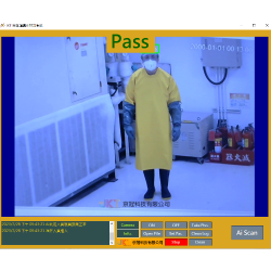
AI Image Recognition for Wearing Protective Gear
-

Facial Recognition Solution- FaceMatch
-

Magnetic Series
-
Fusion series(Flex-Eye)
-
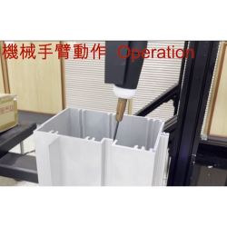
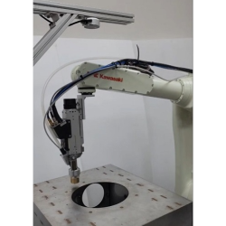
Kawasaki robot doing glue application
-
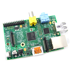
Raspberry Pi
-
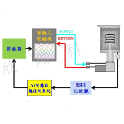
CRYO PUIMP 壓縮機AI智慧節能控制系統
-
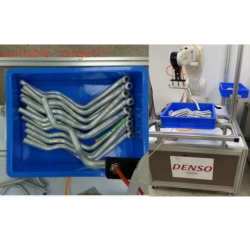
Bent pipe picking
-
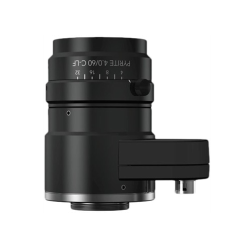
Schneider Industrial Lens
-

NVIDIA 戰情室, AI分析 / Omniverse 數位孿生
-
CX.I series
-
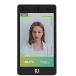
Facial Recognition & Thermographic
-
Fun2D YinYang Eyes Machine Vision Solution
-

ARS(AI Review System)
-
PLC
-
Kawasaki robot on stud welding
-
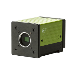
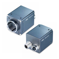
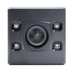
Industrial AI Camera
Highest Rated Products
-
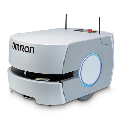
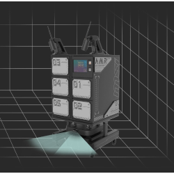
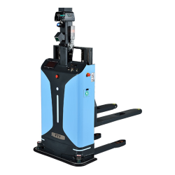
Autonomous Mobile Robot
-
SMR 250 / 1000 series AMR
-
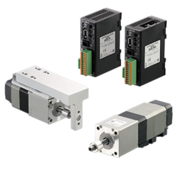
DRS2 Series Compact Electric Cylinders with Absolute Encoder Stepper Motors
-
Delta Industrial Automation
-
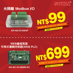
Special exhibition price - Isolated Universal I/O Module AR-403-IO-0404P & Programmable Logic Controller (WEB interface PLC) AR-401-IO-0808R-RX
-
Helios2+ Time of Flight (ToF) IP67 3D Camera
-
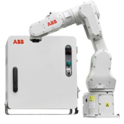
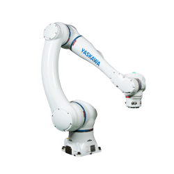
IRB 1100 Articulated robots
-
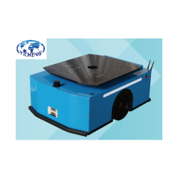
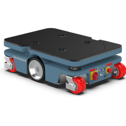
Lift Type Automated Guided Vehicle
-
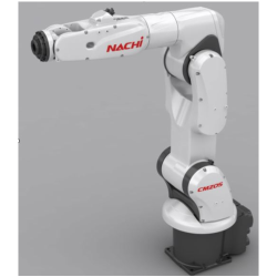
Multi-Axis Robot
-
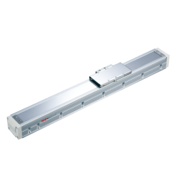
Nano-level linear motor module
-
Collaborative Robot HC Series
-
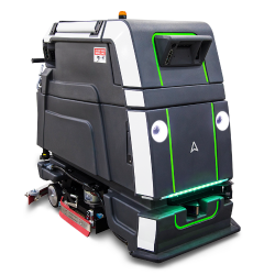
Avidbots Neo 2.0
-
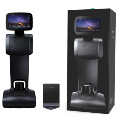
Robot Temi
-
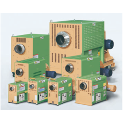
Hot-air generator
-
LE MINI SENSOR AIR HEATER
-
Static Remover
-
Side Running Conveyor
-
All kinds of AGV/UGV/AMR
-
Belt type Electric Actuator/ Screw rod electric slide table actuator
-
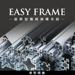
EASY FRAME system
-
Cooperative Robot
-
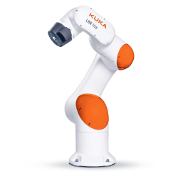
LBR iisy Cobot
-
AMR-AI-Logistics Robot
-
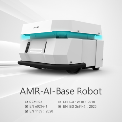
AMR-AI-Base Robot
-
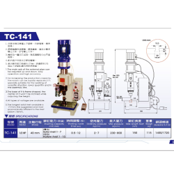
Pneumatic Riveting Machine
-
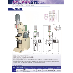
Hydraulic Riveting Machine
-
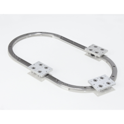
Saibo Precision V-Rail Linear & Rings
-
Smart Forklift CDD14
-
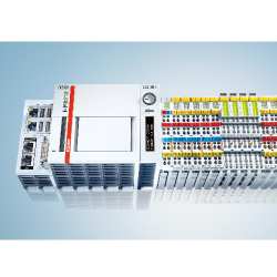
PC-based controller
-
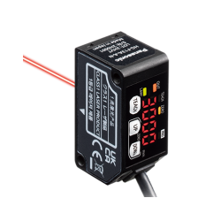
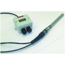
Panasonic Compact & Long Range Laser Distance Sensor


