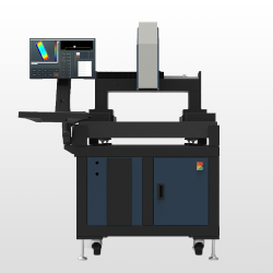
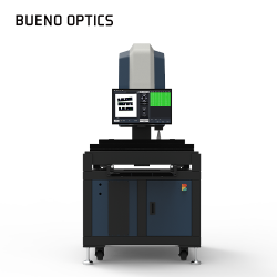
Intelligent Wafer Thickness Measurement System
Model: 5AT3
Category: Smart Manufacturing
Exhibitor: BUENO OPTICS CO., LTD.
Booth No: L701
Characteristic
Intelligent Wafer Thickness Measurement System
For semiconductor wafer grinding, thinning process or chemical vapor deposition (CVD), epitaxy, and film forming process, there will be a need for thickness monitoring; it also provides accurate measurement of wafer bow, warpage or thickness uniformity generated during the analysis process.
Using a non-contact capacitive displacement sensor module or a white light conjugate foci displacement module, together with a high-precision displacement platform for full-plane scanning, the multi-point wafer thickness real-time measurement data can be obtained within a few seconds.
In addition, an optional wafer diameter measurement module can measure the wafer size accurately and quickly by using optical contour image processing technology. The system can also integrate four-point probes to measure surface resistivity and P/N TYPE to achieve multi-function measurement in one machine. The built-in point path of the software includes 5, 9, 37 points and a custom point path to achieve multi-point measurement information of the wafer; the system can also read the Wafer ID information of the wafer. It is equipped with square porous ceramic vacuum suction cups and positioning fixtures, which are suitable for various shapes of objects to be sided, and are compatible with 2”4”5”6”8”12” wafer measurement.
Other Products
-
Engineered for Speed QA/QC and R&D Solution
-
Intelligent Optical Wafer Surface Defect and Height Variation Inspection Equipment
-
Intelligent optical inspection machine
-
Automated Optical Recognition For 2D Measurement
-
Intelligent automatic optical 2D image contour size measurement equipment for large workpieces
-
Recycling machine
-
2D Intelligent Optical Measuring Instrument(85mm x 55mm Small Platform)
-
Non-Contact 3D Surface Profile Optical Measuring Instrument
-
2D Intelligent Optical Measuring Instrument
Products you may be interested in
-
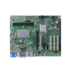
IMB-M47H Industrial ATX Motherboard
-
Industrial Control RS485 Series
-

Restaurant Meal Consumption Solution
-
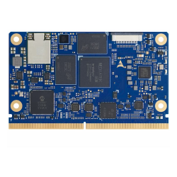
LEC-MTK-I1200 Computer-on-Module
-

Guide to SOYAL Security Communication (SSC)
-

701ServerSQL New Features
-
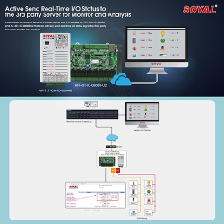
Active Send Real-Time I/O Status to the 3rd party Server for Monitor and Analysis
-
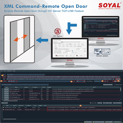
XML Command – Remote Open Door~
-

701Client Auto Send Email Notification Setup
-
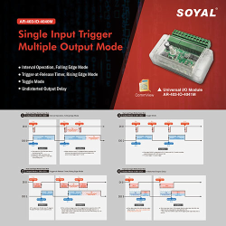
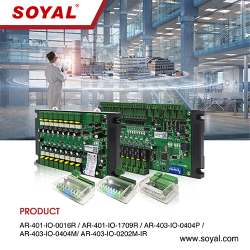
AR-403-IO-0404M - Single Input Trigger Multiple Output Mode
-
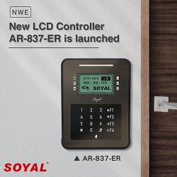
New LCD Controller AR-837-ER is launched
-

MicroRAN All-in-one 5G Private Network Solution
-
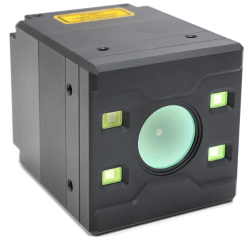
Helios2 Wide 3D Time-of-Flight Camera
-
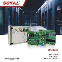
Centralized Multi-door Controller (8-door with uninterrupted power supply(UPS) system)
-
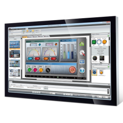
PanKonix Series-HMI Panel PC
-
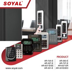
RFID Proximity Controller-Enterprise Series (E Series)
-
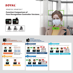
Function Comparison of Face Recognition Controller Versions
-
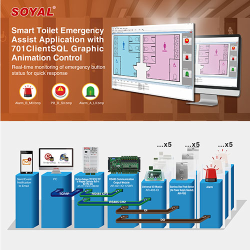
Smart Toilet Emergency Assist Application with 701 ClientSQL Graphic Animation Control
-

SuperCAT - Software-defined EtherCAT Motion Controller
-
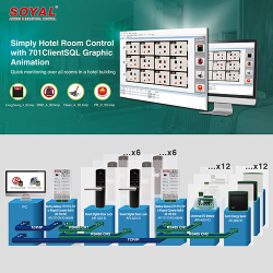
Simply Hotel Room Control with 701ClientSQL Graphic Animation
-

Smart Direction Recognition for Parking Lot Solution AR-403-IO-0404M
-
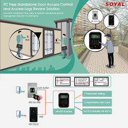
PC Free Standalone Door Access Control and Access Logs Review Solution
-
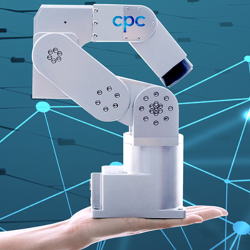
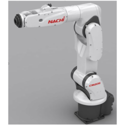
DB0 6-axis robot
-
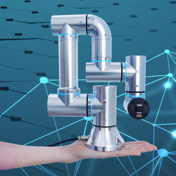
S0 6-axis robot
-
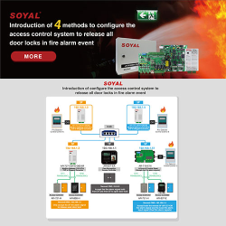
Introduction of 4 methods to configure the access control system to release all door locks in fire alarm event
Highest Rated Products
-
Autonomous Mobile Robot
-
SMR 250 / 1000 series AMR
-
DRS2 Series Compact Electric Cylinders with Absolute Encoder Stepper Motors
-
Delta Industrial Automation
-
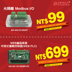
Special exhibition price - Isolated Universal I/O Module AR-403-IO-0404P & Programmable Logic Controller (WEB interface PLC) AR-401-IO-0808R-RX
-
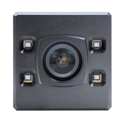
Helios2+ Time of Flight (ToF) IP67 3D Camera
-
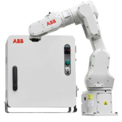
IRB 1100 Articulated robots
-
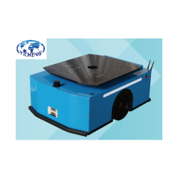
Lift Type Automated Guided Vehicle
-
Multi-Axis Robot
-
Nano-level linear motor module
-
Collaborative Robot HC Series
-
Avidbots Neo 2.0
-
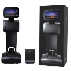
Robot Temi
-
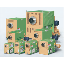
Hot-air generator
-
LE MINI SENSOR AIR HEATER
-
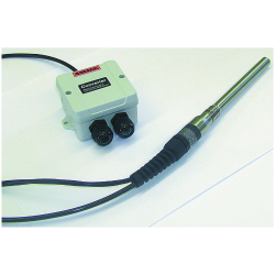
Static Remover
-
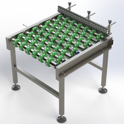
Side Running Conveyor
-
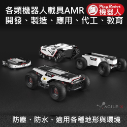
All kinds of AGV/UGV/AMR
-
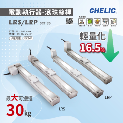
Belt type Electric Actuator/ Screw rod electric slide table actuator
-
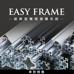
EASY FRAME system
-
Cooperative Robot
-
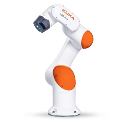
LBR iisy Cobot
-
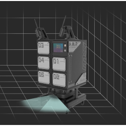
AMR-AI-Logistics Robot
-
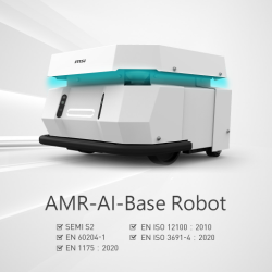
AMR-AI-Base Robot
-
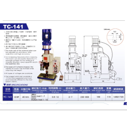
Pneumatic Riveting Machine
-
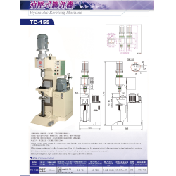
Hydraulic Riveting Machine
-
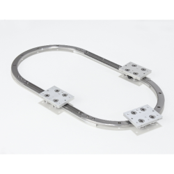
Saibo Precision V-Rail Linear & Rings
-
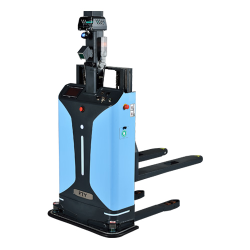
Smart Forklift CDD14
-
PC-based controller
-
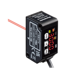
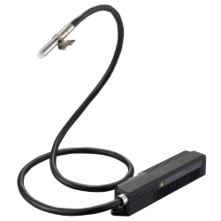
Panasonic Compact & Long Range Laser Distance Sensor


